Multi-material 3D fabrication at nanoscale has been the holy grail of nanotechnology and a key enabler for the development of new technologies, including photonic, electronic, and biomedical devices.
Professor Chen Shih-Chi and his team, in collaboration with Professor Zhao Yongxin from Carnegie Mellon University’s Department of Biological Sciences and Professor Zhao Ni from CUHK’s Department of Electronic Engineering, have developed a 3D nanofabrication platform that for the first time realises multi-material fabrication, meaning it is able to make a great variety of materials, including metals, alloys, semiconductors, polymers, ceramics and biomaterials at a record-setting resolution of 20 nanometers, and a light patterning speed of 300 mm3/hour, three orders of magnitude faster than conventional serial fabrication systems that are currently used in the commercial world.
The achievement has recently been published in the journal Science, affirming its status as a technological breakthrough that leads nanoscale 3D printing into a new era.
“A major challenge in nanotechnology is to fabricate complex 3D structures with materials beyond polymers and noble metals, which was previously limited by photo-initiated chemical reactions. Based on the unique surface properties and nano-structures of the femtosecond light sheet-patterned hydrogel found by our team, we proposed a kinetically controlled nano-assembly process to substitute the conventional photo-reactions. As the strategy mainly relies on the physical properties of functional materials, such as sizes or hydrophilicity, the limit of material selections can be entirely overcome. Next, by shrinking the patterned gel substrate in acid, we can easily break the diffraction barrier,” said Professor Chen.
Fabrication of large-scale woodpile structures: (A) 12-layer woodpile structure of florescent polystyrene (top view, stitched from 16 sub-images due to the limited microscope field of view); (B) zoomed-in view of (A), where the inset shows a 3D fluorescent image of the structural details in the selected area; (C) cuboid woodpile structure of florescent protein; (D) O-shaped 3D woodpile structure of CdSe.
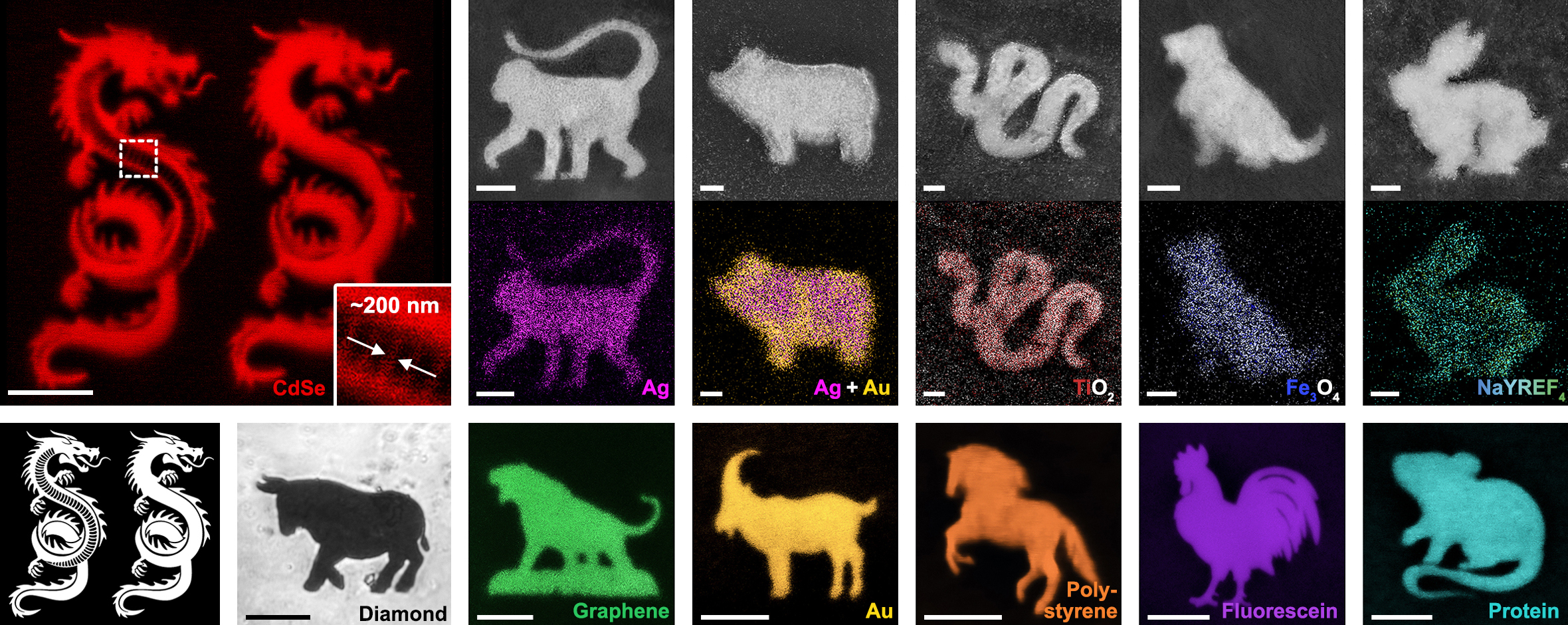
Demonstration of material variety via 12 Chinese zodiac animals, including fluorescent image of two dragons of CdSe quantum dots (QDs) without shrinking (the inset shows a resolution of ~200 nm); SEM (top) and EDX (bottom) images of a monkey of Ag; pig of Au-Ag alloy; snake of TiO2; dog of Fe3O4; rabbit of NaYREF4; optical microscopy image of an ox of diamond; fluorescent images of a tiger of graphene QDs; goat of fluorescent Au; horse of polystyrene; rooster of fluorescein; and mouse of fluorescent protein.
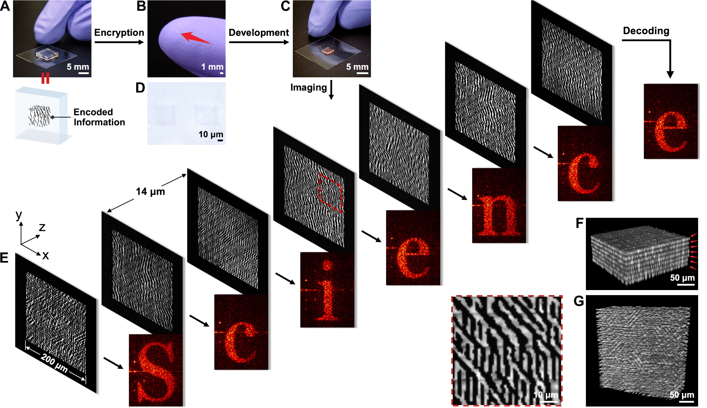
Demonstration of optical storage and encryption: (A) an expanded hydrogel patterned with designed information; (B) the gel in (A) after fully shrinking and dehydration to realise physical encryption; (C) the re-expanded gel is deposited with CdSe and developed to decrypt the stored patterns; (D) Optical image showing two encrypted seven-layer hologram patterns in (B); (E) Fluorescent images of the decrypted holograms, decoding the word “Science”; and (F, G) 3D views of the decrypted holograms.
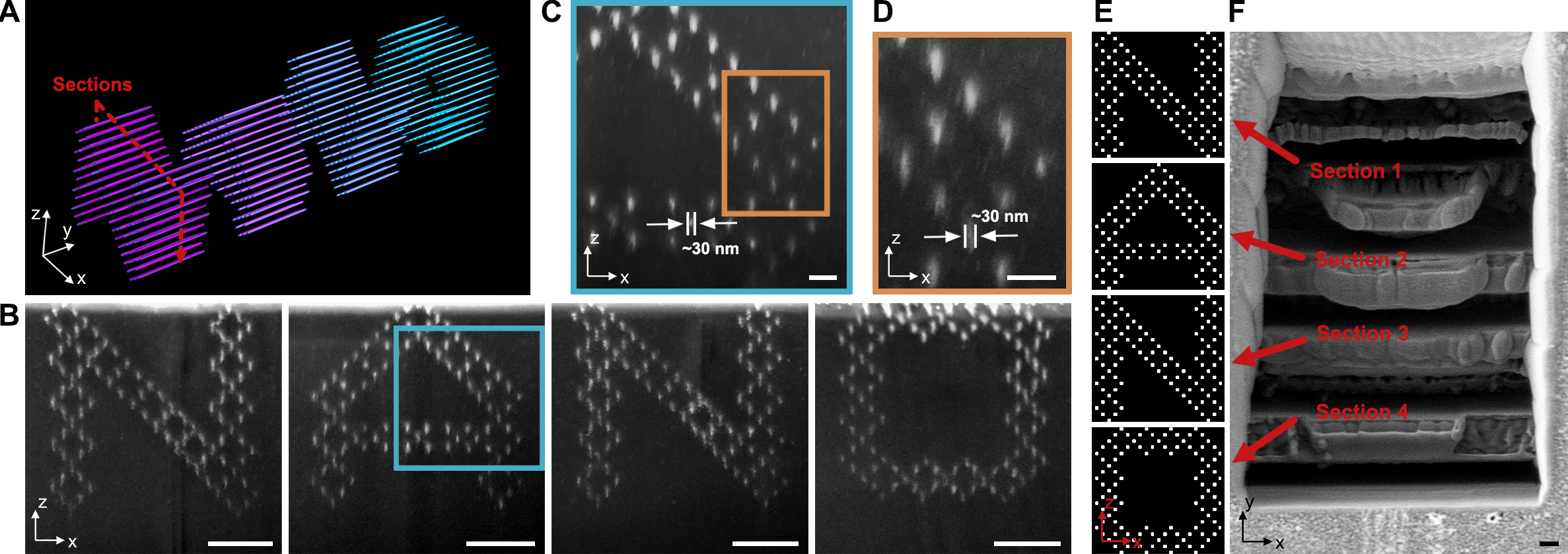
Nanostructures demonstrating minimum feature sizes. (A) 3D model of a nonconnected “NANO” structure comprised of arrays of parallel nanowires; (B) SEM cross-sectional images of the “NANO” structure cut by a focused ion beam (FIB); (C) zoomed-in view of the letter “A” in (B); and (D) zoomed-in view of (C); (E) Four cross-sectional patterns of the “NANO” structure (in the x-z plane of (A)); (F) SEM images showing the trenches of the gel sample opened by an FIB-cut, where the positions of each letter are labelled. All cross-sectional images were taken at a substrate tilt angle of 52°.
The full text can be found at https://www.science.org/doi/10.1126/science.abm8420.
CUHK Press Release: Click here!
MIT Technology Review China: Click here!